• You can now help support WorldwideDX when you shop on Amazon at no additional cost to you! Simply follow this Shop on Amazon link first and a portion of any purchase is sent to WorldwideDX to help with site costs.
  • The Retevis Holidays giveaway winner has been selected! Check Here to see who won!

69610Z Ranger SSB receive problem

Smokinone

WDX-3820
Jun 24, 2020
848
1,074
153
Southern Nevada
I have received a lot of helpful advice on a few radios here, and am now reaching out for some help on another radio please.

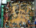
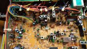
I have been trying to align this radio, a 696 Ranger. I have the PLL freq's aligned but on LSB I have to tune down to 27.384 to receive 27.385. Even then it is distorted. AM is fine for X-mit and RX. USB seems to have the same issue as when I key up another radio into a dummy, I have to tune down to about the same 27.3845 to get a somewhat clear audio. Is there an area to find such a goofy issue. I have 10.240 on the VCO, and, as mentioned, all the freq's are in line with the alignment.

Radio is stock, TR39 removed, that will go back. I have 2 reliable 8 digit frequency counters that I regularly check with a 10K reference. The Victor VC3165 is a little more sensitive than the B&K 1805, but they both agree on the frequencies being read.

Further there doesn't seem to ba any output on LSB, and very low output on USB, while AM is fine.

Radio has been sitting for some time and when I initially hooked up the power, radio turned off, I heard a little pop. Not sure what that was about, but it only did it the once. Probably nothing to do with it, but I never heard another radio do it that I can recall.

Thanks for any help with this. Never had this happen before when aligning radios.
 
Last edited:

Listening to another radio tuned with the same counter, lsb is on freq.
With this Ranger, to get 38 lsb tuned, the VCO alignment for TP3 is 16.68718, and should be 16.6875. Goes through all the frequencies that way.
No mods to the radio, clarifier is stock.

The 15.360 X-tal is reading 15.370. Could this possibly cause the receive to off by the .0003-4 when the VCO is aligned correctly?

What I get on the radio freq counter is 27.3846 to receive correctly with the clarifier to the left.

Another funny thing is that transmitting on AM, I get 27.185 reading at the antenna output, USB 27.18848, keyed 2 tone audio, and LSB I show 27.1828. I think that should be correct, 2 up, 2 down essentially.

I also noticed the VCO chip had been re-flowed, so I don't know if this was an issue in the past. I bought this radio some time ago and am just getting it out of the cabinet. I have replaced a few of the electrolytic caps, and they were all good and within tolerance.

Perhaps a clarifier unlocking to check and see if it pulls the rx and tx together? I am at a loss.

Thanks.
 
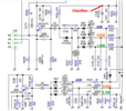
Sounds like you have "lost" the 8 volts you need for the Clarifier on LSB.

So, an easy check would be to see if the Clarifier pot itself - measure the same voltages across all its leads when in AM or USB or LSB.

IF the voltages are the SAME for every mode off the Clarifier header on the main PCB - then we have to think about a steering diode make have blown open.

Else if any of the voltages show a dip - then think about it this way:

The power that goes thru the clarifier is getting pulled down - but yet (or should) shows power at the Pot for it to work, then suspect you have a loading issue, which could be from a bad cap (unlikely for this case because the other modes would also load down this way) a bad header - shorted trace, or a blown diode showing shorted.

The Shorted diode would be in the MODE selector - but it can affect the Clarifier because you "lost" voltage from the clarifier pot - so the system can't power the oscillator unless you provide power for it - which sounds like what the clarifier is trying to do.

That may mean a blown diode in a PACKAGE - which is quite common -but you still have to get your ducks in a row first.
1643566224279.png
1643566707172.png
I hope this information helps...​

It could also be something as simple as a TX RX condition where the Fine Clarifier section is adding to the mess by still getting power - which if the unlock was done right would always be there for it but you wouldn't have TX power getting shoved in there 2X bypassing the Fine altogether.

Just some things to think about...
 
Thanks for being here Andy.


No clarifier mod in this. The limiter was removed and is now back in place.

I have 8.76V to 8.85V on the supply to the clarifier pot on any mode as the clarifier is worked.
There's a white and black wire coming from the pot, I haven't traced them out yet but...
The white wire in any mode is 4.92V to 8.73V
The white wire in any mode is 4.92V to 5.96V

Funny I was just looking at this circuit as your reply came in. Not too sure what it does totally, I was just running down the traces to see where they ended up.
F696_1.jpg
 
Checked the "mode" switch and have 9V feeding, and going out on the switch as it is rotated or switched.

The radio is essentially a 959 Galaxy with 1 more digit on the freq counter, a few buttons instead of switches. And it has a flag.
 
The board it can hold - can go a lot more channels - sorry for the "extra data".

So ok, the TP3 If seems "low" - but is not deviated 455kHz like you'd have something missing.

So you have to turn down (load up) The Clarifier to even get the thing to slide down low enough - still leads me to the bunny hole of the Clarifier.

To bring the frequency down - you have to ADD voltage to force the capacitive barrier of the Varactor up in value - slowing down that tank oscillator

But you say the voltage doesn't change (you can rotate thru the range but it seems high - 8 V is a bit much) you list two white wires, one of these white wires is correctly working 4.5 to as high as 6V - which is the working range of the Varactor it goes to. So one of these wires is working right.

When you located this wire - did you do a TX to RX switchover to observe this on the Clarifier output (Wiper arm)? A small rise / fall - even 0.4V (4 tenths of a volt) can indicate there is a problem.

So if the Clarifier is "stock" the TX side receives power thru D63 in TX mode, but in RX mode R115 and D41 - are in play - so if I'm not getting this right - I'll need to see a pic of the board to make sure I'm guiding you right.

So I'd locate R115, it's a 47 ohm, usually right near the Front panel - by header J10.

Since this board is capable of a lot of stuff that can get us jailed in certain countries, they put jumpers in spots that add to the WTF moments when tracking down this issue.​

What you need to check - is both sides of this resistor in RX - then in TX mode.

Why? A hunch the Clarifier is wired wrong or the "steering diode" D41 - may be shorted - LOADING the TX line - leaving you to tune one direction - while the RX mode supplies power correctly, but in TX - it pulls off power in the other direction trying to power RX - but when you get RX to work there - something isn't right.

IT could also mean the wiring on the pot is wrong - or a jumper is not set right.

We're not done here, the same line that feeds that R115 (RX power) also goes to the RF Gain control. So if you're having Receive issues, the RX power line might be getting pulled down by something ON the line to this section.

If I'm rambling - let me know I'll stop so others can come in here and help you figure out this mess.
 
Clarification (no pun) is needed on the clarifier pins:
The blue wire is the source 8V, goes to F1 on J9
The white wire, F2 on J9, in any mode is 4.92V to 8.73V
The black wire, FG on J9, in any mode is 4.92V to 5.96V
They are all plugged into connectors on the main board or clarifier board.
Of those, the one that is 4.92 - 5.96 V is the grounded leg of the clarifier, blk wire, according to the schematic for the 959 (same board).
The white wire or F2 has a range of 4.92 to 8.74 one end to the other.
Sorry for the double use of white wire. Was up at 2:30am after not much sleep playing with this thing. I feel like the Scarecrow sometimes.

PLL alignment for AM at TP3 is 16.27000, USB is 16.27250, LSB is 16.26751. L20, 21, 22 respectively. L22 was/is very touchy to get set.

After setting those parameters, receive at USB 27.3840 to get clear audio from a radio tx at 27.385, and LSB 27.3847 to get understandable audio. Then when switching from mode to mode, the LSB at TP3 goes to 16.26738. It doesn't seem to hold it's setting. Now after another aligning on LSB, switch the mode to AM, USB, back to Am and back again to LSB. Now LSB is at 16.26762 without touching the pots.

I'm wondering if the L22 needs to be replaced, but that wouldn't explain the basically same issue with USB. Now I left the LSB at 16.26754, best I could get, I keyed the other radio and the TP3 reading went to 16.26743...without moving anything on the radio.

I thought for a moment I had a revelation as TP3 post was a cold solder joint. I fixed it but no change.

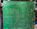
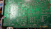
fd1-1.jpgfd1-2.jpgfd1-3.jpgfd1-4.jpg

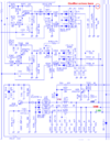
Here is the schematic and service manual I'm working from.

R115 on this board is just below X1. There is an R113 in the area you state. One side is 9V RX, keyed 0.065V...other side 8.8V RX keyed 0.065V.

I learn from everything you say HA. Just the steps you outline are helping me to find my way around so to speak.

I spent a lot of my day cleaning my desk area as somehow the shorting bar got lost. And after cleaning everything up, which really needed it, I still didn't find the little board. I checked the wash and my jammy pockets, everything i could think of...then I happen to look at my soldering iron holder, and there it was nestled in the back of the opening. Things just have to be difficult for me.

Thanks much HA, as always. Some of what I said might not make sense, but I try my best.
 

Attachments

Last edited:
Oh ok! J9 - got it, now I have to look for a different schematic...959 - but I also wanted to caution you, and unless you have a hot-air station - this is going to be a labor of love going over nearly every solder joint on these boards.

Go back and look for the "white wash" - their cleaner rinse - they certainly did not do (more like doo) a good job on the rise and clean.

This is a sure sign of cold - poor soldering joints - and possible component damage, referring to the clarifier pot.

You might have to do up a 10K pot to replace the one they seem to have really washed out and lost some if not most of the composition.

Why?

The pots' output voltages are way too high.

Reheating the solder joints following the traces back to the IF by the VCO is where I would continue....

In TX see if you can even get the 10.695 side of this, it seems that you have to tie LSB to some extreme range of one of the IF's - your comment about USB being understandable while LSB (the inverted one) is having a harder time "decoding" tells me something localized to the two IF's you're switching between - the USB seems ok, the LSB is not - but in order to even get close you have to use an extreme measure on the LSB side.

So that takes me here...

1643634425969.png

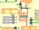
You have TP5 and TP6 for Am/SSB IF 10.695/10.625 stuff

1643634571059.png
1643634638802.png

LSB is handled thru L25/L22 - you are looking at L22 - but L25 is also used but in TX - if something in the TX side throws you off, as in - tuning is easier for the TX than RX you can find yourself chasing after an obvious problem, but you also have to go back and look for "What IS Causing This Obvious Problem?"

So does that mean a goofy Mode switch or is the Clarifier sending the wrong voltage?

Well, if you don't mind - locate D51, D52 and D53 - by those L22 - L20
Measure voltage on the UNBANDED side - all should be equal - but ONLY for that mode that coil represents - so the mode should have a voltage, the other modes it would not - and see if there is a difference in the reading off those diodes in the modes they are supposed to be on.

The diodes are to steer power to the VCO for that mode,

Thx - have several schematics for Ranger/Galaxy boards but to which it's own???

Now I can work with what you are using.

1643636366771.png
 
Last edited:
  • Like
Reactions: tecnicoloco
So, in the above - I'm trying to isolate your "low" condition - which really - is "High" because somehow the Varactor appears to be getting a different voltage.

Seeing that you have to chase downwards - the frequency - seems to indicate the Selector (MODE) side that powers that specific section the Clarifier then "offsets" using a voltage from itself - sends power thru one of this set of coils for that mode which tunes this oscillator - power from one - to turn it on, then the Varactor is tuned by the difference between the two to develop the capacitor to make it "ring" at the specified frequency.

So, this would also affect the DECONVERSION side too. You don't seem to have this problem in USB - you say it works, But LSB uses the same principle - but in THE RX mode the TP3 has to shift to work the deconversion further down the chain - so you're hearing the effects - but is the IF strip seeing/switch off the right section in the SSB mode? I think you're ok that way...

But - Did you disconnect the Frequency Counter for a quick loading check?

Why? Well, the Frequency counter sees the IF offset from this same section - but to display it - it must use the mode selected - send power to a pin - to tell the counter to display the corrected frequency - two pins 5 and 6 are used for this.

Got a snapshot of the wiring locations else they usually use the Header J21 (Frequency) J22 for 8V and switching info...

  • your problem seems to be the RX side
  • You did ask about "unlocking"
  • Then all you need to do is remove R113/D68
  • Solder 8V constant (thru R113 to reduce the tuning headaches) to re-establish the Clarifier pots constant 8V source.
    • R113 can have the leg that is away from the J9 connector (board component side up front panel facing you - it would be right leg) - lift it up and solder your 8V wire from JP200 or JP190 to freed/lifted leg of R113.
  • Locate C1 and C2 on main PCB by F1 and F2 (Where your Clarifier goes)
  • Does it have a solder short?
  • It should you wouldn't have USB if that was the condition.
 

Attachments

  • 1643638145547.gif
    1643638145547.gif
    83.3 KB · Views: 8
Last edited:
  • Like
Reactions: tecnicoloco
In TX see if you can even get the 10.695 side of this, it seems that you have to tie LSB to some extreme range of one of the IF's - your comment about USB being understandable while LSB (the inverted one) is having a harder time "decoding" tells me something localized to the two IF's you're switching between - the USB seems ok, the LSB is not - but in order to even get close you have to use an extreme measure on the LSB side.
I haven't been able to locate a specific service manual for the 696FD1.

Actually the receive side of USB has to be tuned down further than the LSB side. Whatever is going on appears to be isolated to the SSB side of the radio, or did. Seems now that both the LSB and USB have to tune down to 27.3840 for clarity on receive. I don't know what caused that change. I have re-seated most of the connectors by unplugging them and re-connecting.

The xmit alignment of the 10.69500 AM (L23), 10.69250 LSB (L24), and 10.69750 USB (L25) all fall into place.

The RX side of the alignment connected at TP3, AM (L20) 16.51000, USB (TP21) 16.51250, and LSB (TP22) 16.50750. All where they are supposed to be. That's what makes it so frustrating.

3.55V on the D50, D51 4.18V, D52 4.18V when set in their respective modes.

  • Locate C1 and C2 on main PCB by F1 and F2 (Where your Clarifier goes)
  • Does it have a solder short?
It does have the shorting wire in place. Thanks for this. I can see a clearer picture now of the circuit I didn't see the correlation until you pointed it out with the diagram and some tracing.

My 8V buss is at 9V. This may be the issue? Q37 is the regulator, a 2SA473, it does appear to be working, I have 13.7 or so to it. D73 is a 7.5 zener tied to it.

I like what you did with the "unlock" on the clarifier. I am going to wake up a bit and give that a try. Certainly can't hurt and may shed more light on the situation.
When I start to dig into your suggestions, I see a lot more and am gaining some understanding that I don't have. In fact, when going through this with you reminds me of my father in law explaining a lot of what is going on. Sadly he has passed, but I am having some aha moments as I follow along.

Thanks a ton for your time and explanations.

J21 & J22...pardon my finger
fd1-J21.jpgfd1-J22.jpg
 
  • Like
Reactions: Handy Andy
Update: More problems

Hooked up the dummy load and transmitted into it while listening on another radio with a DL on it to see if the X-mit was in line with the receive. I get a squeal on USB into the receiving radio and an output of about 12 watts swing. On LSB no audio at all into the receiving radio and show a swing of about 2-3 watts output. No issue with AM.
Still haven't done the unlock on clarifier.

Thanks
 
  • Like
Reactions: Handy Andy
This is telling me as you work on it, the radio is akin to bad soldering - when USB and LSB start to line up low or high - near their limits - the alignment originally done and where you have to set it now will be different.

Each joint you reheat - understand that the resistor or capacitor or any part used, uses a tinned - or supposed to be tinned - lead with solder - but they don't tell you the type of solder they used to tin it - lead or silver or antimony alloy - so some solder reheating and rework is needed to re-tin the leads to accept the new "different alloy" solder. Else the joint will work as a highly resistive one until the wetting is good enough to make the joint look like a soldered joint as the proper connections

Since you're in a RF/IF area - this will be a problem for any type of soldering system, affects Discrete and SMD as well.
 
Thanks HA. I will continue to play around a little and see where it goes. Do some voltage checks etc. I have the CBC Galaxy Service manual, it goes a little further than the regular service manual. Forgot I had it. I'll do some reading and testing.

There's a whole lot more to deal with on these SSB vs AM radios when something goes wrong. Learning as I go.

I appreciate the time spent.
 
Update:

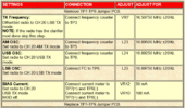
OK, I found the problem. I was using the CBC GALAXY Service Manual Second Edition.

When aligning the carrier oscillator offsets, according to this manual, they want you/us to use TP6 for adjusting same.

I was looking over the same adjustments for Oscillator alignment for the Galaxy DX959 and they use TP5 for those adjustments. Using the TP5 to make the adjustments everything fell into proper alignment with great receive and transmit, and on frequency.

By the way, I have the factory manual for the Galaxy 2547 and it also shows TP6 as the pint of adjustment further complicating matters.

An truly frustrating experience.

Thanks again HA, I guess I should pay better attention, or at least use a correct factory manual. It appears the DX959 is correct for the TR696-FD1
 
  • Like
Reactions: NZ8N and Handy Andy

dxChat
Help Users
  • No one is chatting at the moment.