You are using an out of date browser. It may not display this or other websites correctly.
You should upgrade or use an alternative browser.
You should upgrade or use an alternative browser.
-
You can now help support WorldwideDX when you shop on Amazon at no additional cost to you! Simply follow this Shop on Amazon link first and a portion of any purchase is sent to WorldwideDX to help with site costs.
-
The Retevis Holidays giveaway winner has been selected! Check Here to see who won!
Cobra 29 LTD Classic FL2 Filter
- Thread starter RCIGuy
- Start date
Last edited:
That's a good sign, so now as long as the TX light is red, double check voltages in the TX section to the readings you should get.Edit When key up the green rx light will turn red to indicate tx.
You're getting there!
The only voltages that are close are the driver and final, the rest are off, not even close. Makes no sense. You dont think #7 dead pin on ic3 is an issue?That's a good sign, so now as long as the TX light is red, double check voltages in the TX section to the readings you should get.
You're getting there!
What voltages are you getting on TR16 when in TX ? The only thing that "could" pull down Pin7 of IC3 to 2v (also only active in TX) while the LD is a high condition (4.7v??) , could be a shorted Base on TR16. The Emitter should be under a volt, the Base should be .7v above Emitter voltage. Collector should be around +8v, again, only in TX.
Ok, i checked TR16 again in TX
B=104.8mv (keeps climbing up)
C=7.67v
E=.798v
I did a test with a resistor across the ex speaker and pa and the "talkback" works fine. First time ive heard anything out of it.
Switched out TR16 c941 with a c945, made no difference
B=104.8mv (keeps climbing up)
C=7.67v
E=.798v
I did a test with a resistor across the ex speaker and pa and the "talkback" works fine. First time ive heard anything out of it.
Switched out TR16 c941 with a c945, made no difference
Last edited:

-----------------------------------------------------------------------------------------

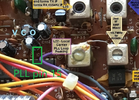
TR16 - E is the Left pin, C is Center pin, B is the Right. B should be about 0.6v to 0.7v above E voltage.
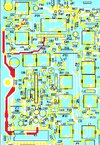
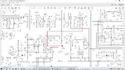
Red trace is from the LD pin (15), to JP2 under the PLL IC, then continues towards the back through R102 (3.3k), to D14 (low LD state disables TX Mixer) and to R62 (2.2k) which provides Bias to TR16. If LD High state, should enable the TX Buffer (or sometimes called TX Pre-Driver), and a LD Low state disables TX.
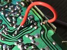
Try this: Remove R102 (3.3k), set aside to put back later (already pre-bent to correct shape and length), and put another 3.3k from the left trace where D14 or R62 are on that trace, to either JP31 (next to L20), or JP32 (feeds +8v TX to Collector of TR16 through L17), or to JP29, next to L17.
This disables the LD lock-out of the TX. See where (if at all) it transmits on what frequency.
Thats what i did. Soldered to D14 and JP31, unless i did it wrong it made no difference at all, went through all the channels with frequency counter and no tx on any channel, still no carrier at all. Thank you for the help, much appreciated.Take the 3.3k you pulled, solder a wire to extend it, I didn't know if you had a 3.3k laying around or in a drawer, or loose. Now try. You can always rebend it back in shape to restore it later.
Please dont judge my soldering, i know its a temperary thing, didnt do an outstanding job on it.
On the upside i can listen to "the bowl" through the dummy load.
Last edited:
Got a spare 941 for TR16?
You did check the Driver and Final for "Good" as in out of circuit and use a tester to show "Good"?
You did check the Driver and Final for "Good" as in out of circuit and use a tester to show "Good"?
dxChat
- No one is chatting at the moment.
-
@ BJ radionut:
HEATHKIT SB220 Used [.20462] - $999.00 : R&L Electronics, Amateur radio store
R&L Electronics HEATHKIT SB220 Used [.20462] - HEATHKIT SB220 MODIFIED TO ONLY WORK ON 6 METERS TESTED, HEAVILY MODIFIEDwww2.randl.com -
-
-
@ benc48:Need help lost my channel chart . Cobra 148 GTL with a 8719 and 11,1125 crystal 26.175 to 28.045 , Need the chart I can fill in the blanks slide 2ck up and 12 kc down
-


